所屬科目:研究所、轉學考(插大)◆電子學
(a). Plot and label the waveform of \(v_o^+\) and \(v_o^-\)
(b). find the amplitude of the sine wave across the secondary winding \(v_s\)
(c). What is the PIV of each diode?
(a) Find the value of the differential gain \(A_d\).
(b) Find the value of the differential input resistance \(R_{id}\) and the output resistance \(R_o\).
(c) If the resistors have 1% tolerance (i.e., each can be within \(\pm 1\%\) of its nominal value), find the worst-case common-mode gain \(A_{cm}\) and the corresponding value of CMRR.
(a) Find the dc collector current of the transistor.
(b) Neglecting \(r_o\), find the midband voltage gain (\(v_o/v_b\)) from base to collector (neglect the effect of \(R_B\)).
(c) Use the gain obtained in (b) to find the input resistance \(R_{in}\) that arises as a result of \(R_B\).
(d) Find the overall gain at midband (\(v_o/v_{sig}\)).
(e) Find upper 3 dB frequency \(f_H\).
(a) midband gain (\(v_o/v_{sig}\))
(b) input resistance connected to the source \(v_{sig}\)
(c) lower 3 dB frequency \(f_L\)
(d) upper 3 dB frequency \(f_H\).
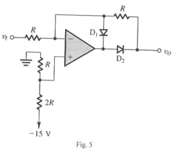
5. Consider ideal diodes in the circuit of Fig. 5. Please plot and label the transfer characteristic curve of the circuit.
 阿摩線上測驗
登入
阿摩線上測驗
登入